MicroLEDs: Lighting The Way To A Solid OLED Competitor

We’re accustomed to seeing giant LED-powered screens in sports venues and outdoor displays. What would it take to bring this same technology into your living room? Very, very tiny LEDs. MicroLEDs.
MicroLED screens have been rumored to be around the corner for almost a decade now, which means that the time is almost right for them to actually become a reality. And certainly display technology has come a long way from the early cathode-ray tube (CRT) technology that powered the television and the home computer revolution. In the late 1990s, liquid-crystal display (LCD) technology became a feasible replacement for CRTs, offering a thin, distortion-free image with pixel-perfect image reproduction. LCDs also allowed for displays to be put in many new places, in addition to finally having that wall-mounted television.
Since that time, LCD’s flaws have become a sticking point compared to CRTs. The nice features of CRTs such as very fast response time, deep blacks and zero color shift, no matter the angle, have led to a wide variety of LCD technologies to recapture some of those features. Plasma displays seemed promising for big screens for a while, but organic light-emitting diodes (OLEDs) have taken over and still-in-development technologies like SED and FED off the table.
While OLED is very good in terms of image quality, its flaws including burn-in and uneven wear of the different organic dyes responsible for the colors. MicroLEDs hope to capitalize on OLED’s weaknesses by bringing brighter screens with no burn-in using inorganic LED technology, just very, very small.
So what does it take to scale a standard semiconductor LED down to the size of a pixel, and when can one expect to buy MicroLED displays? Let’s take a look.
All About the Photons

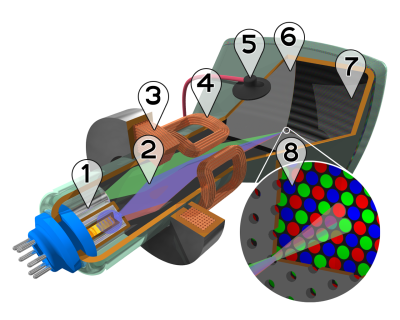
The most important property of a display is of course the ability to generate a sufficient number of photons to create a clear image. In the case of CRTs, this is done by accelerating electrons and smashing them into a phosphor layer. Each impact results in a change in the energy state of the phosphor molecule, which ultimately leads to the added energy being emitted again in the form of a photon. Depending on the phosphor used, the photon’s wavelength will differ, and presto, one has a display.
The reason why CRTs are rather bulky is because they use one electron gun per color. While this is fairly efficient, and the use of electromagnetic controls make for impressively fast scan rates, it does give CRTs a certain depth that is a function of display dimension. An interesting improvement on these classical CRTs came from Canon and Sony in the form of SED and FED, respectively during the early 2000s. These display technologies used semiconductor technology to create a single electron gun per pixel, which would fire at the phosphor layer, mere millimeters away.
By that time LCD technology was already beginning to become firmly established, however. Unlike like the somewhat similar plasma display technology, SED and FED never made it into mass production. Even then, LCD technology itself was going through some big growing spurts, trying to outgrow its early days of passive matrix LCDs with slow response times, massive ghosting and very narrow viewing angles using primitive twisted nematics (TN) panels.
Even though LCDs were clearly inferior to CRTs during the 1990s and into the early 2000s, what LCDs did have, however, was thinness. Thin enough to be put into mobile devices, like laptops and the ‘smart assistants’ of the time, such as personal digital assistants (PDAs). As LCDs gained features like active matrix technology which removed most ghosting, and new liquid crystal alignments (e.g. IPS, MVA) that improved viewing angles, so too did their popularity grow. Clearly, bulky displays were to be a thing of the past.
The Curse of the Backlight

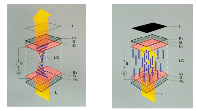
An LCD has a number of layers that make it work. There is the liquid crystal layer that can block or let light through, there are also the color filters that give pixels their colors, and the TFT control and polarization layers. Most LCDs use a backlight source that provides the photons that ultimately reach our eyes. Because of all these layers in between the backlight and our Mark I eye balls, quite a lot of energy never makes it out of the display stack.
In the case of a ‘black’ pixel, the intention is to block 100% of the backlight’s energy in that section using the LC layer. This is both wasteful, and since the crystals in the LC layer do not fully block the light, LCDs are incapable of producing pure blacks. While some LCD technologies (e.g. MVA) provide better a much better result here, this comes at compromises elsewhere, such as reduced response time.
This illustrates the most fundamental difference between a CRT display and an LC display: a CRT is fundamentally dark where the electrons don’t hit. SEDs, FEDs and plasma displays are also self-illuminating, as is OLED. This is a crucial factor when it comes to high dynamic range content.
With the move to LED-based backlights for LCDs, the situation has improved somewhat because an LCD can have different backlight sections that can activate separately. By using more, smaller LEDs in the backlight the number of so-called dimming zones can be increased, making darker blacks. You can see where this is going, right?
The Future is Self-Illuminating
After decades of display technology evolution, the factors which determine a display technology’s popularity essentially come down to four factors:
- How cheaply it can be produced.
- How well it reproduces colors.
- How well does it scale.
- How many use cases does it cover.
In the case of LCDs over CRTs it was clear why the latter couldn’t compete, and why plasma screens never made a big splash. It also makes it clear that – as demonstrated by e.g. Samsung exiting the LCD market – LCDs have hit somewhat of a dead end.

MicroLEDs were invented over twenty years ago, and while e.g. Samsung’s The Wall is seeing limited commercial use, the most exciting development will probably come this year, with MicroLED TVs that fall into the ‘affordable’ range appearing, assuming one’s target is a 76″ MicroLED TV for roughly what an early plasma display would have cost.
Smaller MicroLED displays are unlikely to appear for a while. Immature manufacturing technologies and the need to reduce pixel pitch even more are the bottlenecks at the moment. This latter point is quickly seen in the specifications for Samsung’s MicroLED TVs to be released this year: they only support 4K, even in the 110″ version. At 50″, 1080p (‘fullHD’) would be about the most one could hope for without sending production costs skyrocketing.
A Matter of Time
As cool as new technologies can be, one cannot expect them to fall off the production line one day, all perfect and ready to be used. Early CRTs and passive matrix LCDs were terribly in their own unique ways . As the technology matured, however, CRTs became reliable workhorses at very affordable prices, and LCDs became pretty tolerable.
OLED technology started off with an optimistic ~1,000 hour lifespan on the early Sony prototypes, but today we see (AM)OLED displays everywhere, from cellphones to TVs and even as tiny monochrome or multi-color screens for embedded applications. With MicroLED having the benefit of being based on well-known semiconductor technologies, there’s little reason to doubt that it’ll undergo a similar evolution.
As MicroLED features higher brightness and longer lifespan that OLED, with lower latency, higher contrast ratio, greater color saturation, and a simplified display stack compared to LCDs, it’s little wonder that MicroLED displays are being produced by not only Samsung, but also by Sony (‘Crystal LED’) and AU Optronics, amidst a smattering of other display manufacturers, and tantalizing promises of small (<5″) MicroLED displays.
We know you like lots of tiny LEDs. Will your love last once they become commonplace?
Post a Comment